Worm Breeder's Gazette 11(4): 115
These abstracts should not be cited in bibliographies. Material contained herein should be treated as personal communication and should be cited as such only with the consent of the author.
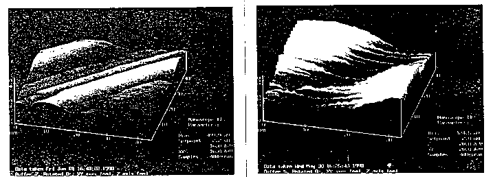
We have been studying C.  elegans microtubules from cellular and
genetic aspects.  Since scanning tunneling microscopy (STM) can
provide atomic resolution of metals and semiconductive surfaces; our
objective is to obtain images of C.  elegans microtubules resolved at
the atomic level.  However, application of STM to biomolecules is
faced with a variety of problems, including poor electrical
conductivity, flexible stability under STM imaging conditions.  In
spite of limitations, recently, impressive images of DNA biomolecules
have been obtained at atomic resolution.
Microtubules (MT) were isolated from 30g of freshly grown N2 worms
according to the procedure of Aamdot and Culotti 1986, and Siddiqui et
al 1989, using cycles of temperature dependent assembly and
disassembly (Shelanski, et al.  1973).  Assembled MT were taken in MT
isolation buffer (containing 0.1mM GTP, 20 M taxol, and 2.0 mM DTE),
diluted tenfold and fixed in glutaraldehyde (0.1%).  The samples were
kept frozen at -20 C, for 4-5 days.  The STM imaging samples were
thawed, and a drop was smeared onto a chip of freshly cleaved HOPG (
highly oriented pyrolitic graphite, Union Carbide), and allowed to air
dry at room temperature.  The STM images were obtained using
'Nanascope II Digital Instruments, California (Sam Howell and C.  Lee,
kindly helped with the STM settings).  All STM imaging was conducted
at atmospheric pressure and at room temperature (22 C).  Two different
STM images of C.  elegans MT are shown here.
[See Figure 1]
Most of our STM scans of MT correspond to one or two microtubules,
but they appear flattened and bent along the seams of the
protofilaments.  The dimensions of alpha and  -tubulin dimer subunits
are about 8 nm, and each protofilament has a width of 4.6 nm.  The
flattening and buckeling of protofilaments along the seams could arise
due to the fixation conditions, or caused by the STM current flow
through the specimen.  At present, we are unable to attribute this
observation to any single factor, and the images of MT do not provide
any higher resolution than conventional electron microscopy using
negative staining.  But it is increasingly possible that one may be
able to resolve individual amino acids or even atoms using STM.  We
plan to continue looking for improved conditions for better STM or AFM
images of C.  elegans MT.
Brief description of
STM:
Scanning tunneling microscopy (STM) traces three dimensional images
of surfaces - even at the level of individual atoms.  Gerd Binnig &
Heinrich Rohrer of IBM Zurich received the Nobel Prize in 1986 for STM
(Refer, e.g.: Scientific American, August,1985).  Briefly in STM, the
'aperture' is a small tungston probe, its tip extremely fine (about 0.
2 nm in width, and may consist of a single atom).  Piezoelectric
controls move the tip within a nanometer or two of the surface of the
conducting sample, allowing an overlap between the electron clouds of
the atom at the probe tip and the closest atom of the sample placed on
the surface.  As a small voltage is applied to the tip, electrons
'tunnel' across this gap, creating a tiny tunneling current.  The
strength of the tunneling current is exponentially sensitive to the
width of the gap (about an order of magnitude per angstrom).
Depending on the substrate, typical currents and voltages are in the
range of nanoamperes and millivolts.  A servo system uses a feedback
control that keeps the tip to substrate gap constant, by modulating
the voltage across a piezoelectric positioning system (Piezoceramic
materials expand or shrink extremely small distances (i.e.  angstroms )
in response to the applied voltage.  As the tip scans the surface,
variations in this voltage, when plotted correspond to surface
structure.
I wish to thank members of Ward lab (Alicia, Andrea, Bill, Bonnie,
Bruce, Jacob, John and Paul); Hameroff Lab (Dolly, Larry, Mohammad,
and Richard); and Sarid Lab (Sam and Lee).